
Introduction#
In this post, we turn our attention to data storage. Data storage is crucial for performing calculations, where input values are stored before processing, and outputs are held afterwards. The most common component for storing data in these scenarios is a register.
Registers#
Registers are at the heart of a CPU. A register is a component that can store a value and hold it until it is needed. In programming terms, it functions similarly to a variable.
To work, a register requires an input value and a load signal that instructs the register to store the input value.
In MHRD, the DFF (D-Flip-Flop) component is used for building registers. The DFF stores an input value and outputs it one clock cycle later. Clock cycles, which determine the speed of a CPU, are managed by a clock component, which we will discuss later. Below is an example of a DFF:
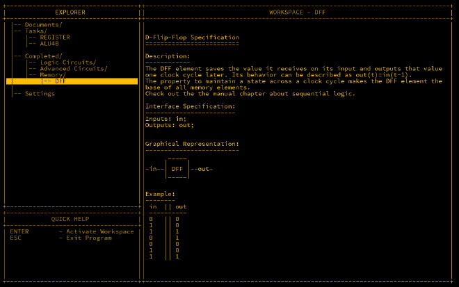
As the documentation suggests, we use DFFs to construct registers. The register takes an input bit and a load signal. When the load is active, the input value is stored in
the register, and the stored value is outputted on the out pin.
The trick is to feed the register’s output back into its input unless the load is active. When load is active, the input value is stored instead. This can be achieved using a
multiplexer (MUX). The wiring is as follows:
Inputs: in, load;
Outputs: out;

Parts:
 d DFF,
 m MUX;

Wires:
 in -> m.in2,
 load -> m.sel,
 m.out -> d.in,
 d.out -> out,
 d.out -> m.in1;
This setup allows the register to store and repeatedly output a value until a new one is loaded.
Register4B#
While a 1-bit register can be useful, storing larger values requires more bits. A 4-bit register can store values from 0 to 15. As we’ve already built a 1-bit register, we can extend this design to create a 4-bit register by using four 1-bit registers.
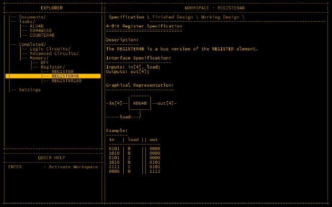
The wiring for a 4-bit register is as follows:
Inputs: in[4], load;
Outputs: out[4];

Parts:
 r1 REGISTER,
 r2 REGISTER,
 r3 REGISTER,
 r4 REGISTER;

Wires:
 in[1] -> r1.in,
 in[2] -> r2.in,
 in[3] -> r3.in,
 in[4] -> r4.in,
 load -> r1.load,
 load -> r2.load,
 load -> r3.load,
 load -> r4.load,
 r1.out -> out[1],
 r2.out -> out[2],
 r3.out -> out[3],
 r4.out -> out[4];
This design also unlocks the REGISTER16B, which is a further extension of this concept.
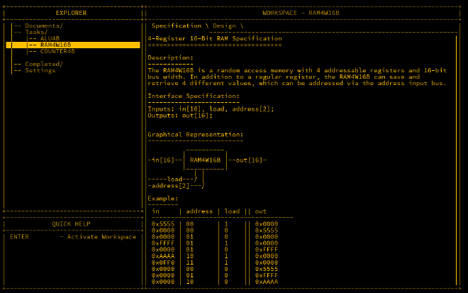
RAM4W16B#
Registers are excellent for CPU calculations, but what if you need to store large amounts of data? The answer is Random Access Memory (RAM), which is essential for most computers. RAM allows data to be written and recalled later, much like registers, except it consists of multiple registers linked together. Each register is assigned an address for reading and writing. In this case, we start small, with four registers.
Understanding Hexadecimal#
If the F values in the example above seem confusing, it’s a good time to discuss hexadecimal notation. While humans count using base-10 (decimals) due to having 10 fingers,
computers, using binary, work in powers of 2. A single bit allows values of 0 or 1, but 4 bits can represent numbers from 0 to 15. In hexadecimal (base-16), values from 0 to 9
are the same as in decimal, but from 10 to 15, letters are used: A, B, C, D, E, F.
You may recall that a byte consists of 8 bits, which can represent numbers up to 255. In hexadecimal, the value 255 is represented as 0xFF. This format allows for more
efficient data representation, especially when dealing with larger values.
Wiring#
Since there are 16-bit inputs, wiring each bit individually would be cumbersome. Fortunately, MHRD provides a shortcut: if an input matches the component’s byte size, it can be wired as a full byte instead of bit by bit.
To store values, we use four 16-bit registers. The in is connected to all registers, but a value will only be stored if the load signal is active. The address is handled by a
DEMUX4W, which routes the load signal to the appropriate register. For output, a MUX4W16B is used to select the correct register based on the address.
The wiring is as follows:
Inputs: in[16], load, address[2];
Outputs: out[16];

Parts:
 r1 REGISTER16B,
 r2 REGISTER16B,
 r3 REGISTER16B,
 r4 REGISTER16B,
 loader DEMUX4W,
 regout MUX4W16B;

Wires:
 in -> r1.in,
 in -> r2.in,
 in -> r3.in,
 in -> r4.in,
 load -> loader.in,
 address -> loader.sel,
 loader.out1 -> r1.load,
 loader.out2 -> r2.load,
 loader.out3 -> r3.load,
 loader.out4 -> r4.load,
 r1.out -> regout.in1,
 r2.out -> regout.in2,
 r3.out -> regout.in3,
 r4.out -> regout.in4,
 address -> regout.sel,
 regout.out -> out;
This design unlocks RAM64K16B, which provides a significant amount of memory.
Conclusion#
Unlocking registers and RAM components marks a major milestone towards building a simple computer. With 64K (65535) bytes of memory, we can handle larger and more complex data processing tasks. Registers are essential for CPU operations, while RAM provides the necessary storage for more extensive computations.