
Introduction#
We’re now in the final stretch of building a fully functioning CPU. But before we reach the finish line, there’s one final piece to construct: the DECODER.
DECODER#
The DECODER takes a 16-bit input and performs basic preprocessing on it.
Decoding the Input#
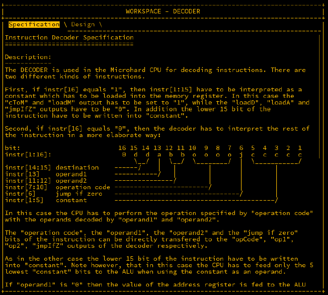
The input is treated as multiple smaller parts rather than one large input. If the MSB (instr[16]) is 1, the documentation specifies that the value stored in instr[1:15] is sent to the memory register. Since the register is part of another section, the first 15 bits are sent directly to the constant output.
When instr[16] is set, a number of flags are activated, which will be handled later. The value of instr[16] is also used to set cToM, which is piped to the appropriate output.
instr[1:15] -> constant,
instr[16] -> cToM,
Destination#
The destination bits control where data is sent. There are three possible destinations: A, M, and D, with each having its own output flag: loadA, loadM, and loadD. Based on the values of the destination bits, one of these flags may be set to 1.
Destination = 00 -> Set all flags to 0
Destination = 01 -> Set only loadA to 1
Destination = 10 -> Set only loadM to 1
Destination = 11 -> Set only loadD to 1
This can be managed using a DEMUX4W that takes a 2-bit input as the selector (sel) and produces four outputs. We set a constant 1 as the input, and the wiring will look like this (further refinement will be required later):
1 -> d1.in,
instr[14:15] -> d1.sel,
d1.out2 -> loadA,
d1.out3 -> loadM,
d1.out4 -> loadD;
Operands, Opcodes, and jmpIfZ#
The next few input bits can be directly routed to their respective outputs:
instr[13] -> op1,
instr[11:12] -> op2,
instr[7:10] -> opCode,
instr[6] -> jmpIfZ;
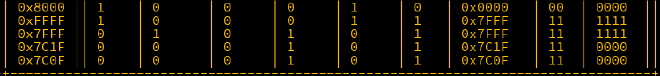
Fixing the load Outputs and jmpIfZ#
At this point, running verification shows that about 60% of the tests pass. The issue lies with the load outputs and jmpIfZ, which are still being set when cToM is active. To resolve this, we introduce MUXes so that if cToM (instr[16]) is set, it takes precedence. Three MUXes (m1, m2, m3) and an OR gate (o) are added to handle the outputs. In the case of loadA, loadD, and jmpIfZ, these are set to 0 when cToM is 1. However, loadM should be set to 1, so we use an OR gate for this.
d1.out2 -> m1.in1,  // loadA
d1.out3 -> o.in1,   // loadM
d1.out4 -> m2.in1,  // loadD
instr[6] -> m3.in1, // jmpIfZ
instr[16] -> o.in2,
instr[16] -> m1.sel,
instr[16] -> m2.sel,
instr[16] -> m3.sel,
m1.out -> loadA,
m2.out -> loadD,
m3.out -> jmpIfZ,
o.out -> loadM;
After updating and running this, the DECODER will be functioning as expected.
CPU#
The final challenge combines all the components we’ve built so far. Here are the five main parts included in the design:
decoder DECODER
// The decoder we just designed, used to handle instruction input.

mReg REGISTER16B
// The Memory Register - used to store addresses in the data RAM.

aReg REGISTER16B
// The Arithmetic Register - for temporary storage of computation results.

pc COUNTER16B
// The Program Counter - determines which address is being accessed in the program.

alu ALU16B
// The Arithmetic Logic Unit - handles the calculations specified by the opcodes.
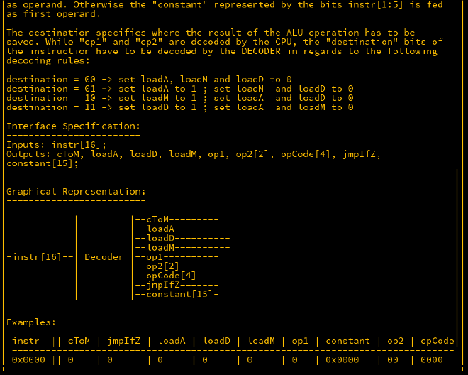
There are several key inputs and outputs to consider:

Externally, we have two RAM units: one for instructions and one for data. The instrAddr and dataAddr outputs request the data at specified addresses, and the instr and data inputs return that data. The in and load inputs for the instruction RAM are not used, but in the data RAM, the in bus is connected to the CPU’s result output, and the load is connected to the write output.
The reset pin is set to 1 to start the program.
Behavioural Specifications#
The CPU uses the decoder outputs to follow the documented behavioural specifications:
instr -> decoder.instr,
- If
cToMandloadMare both1, theconstantoutput must be loaded intoMR:
This can be simplified: whenever cToM is 1, the constant is loaded into MR. If loadM is 1, it will load the value into MR. A MUX16B (m1) will handle this.
decoder.cToM -> m1.sel,
decoder.constant -> m1.in2[1:15],
m1.out -> mReg.in,
decoder.loadM -> mReg.load,
- If
loadMis1andcToMis0, the result of the ALU must be loaded intoMR:
alu.out -> m1.in1;
- If
loadAis1, the result of the ALU must be loaded intoAR:
decoder.loadA -> aReg.load,
alu.out -> aReg.in;
- The
writeoutput of the CPU must have the same value asloadD:
decoder.loadD -> write;
- The
opCodeoutput of the decoder must be fed into the ALU:
decoder.opCode -> alu.opCode;
- If
op1is1, theconstantmust be fed into the ALU as the first operand. Otherwise, use the value fromAR:
A MUX16B (m2) will select between these two sources.
decoder.op1 -> m2.sel,
aReg.out -> m2.in1,
decoder.constant -> m2.in2[1:15],
m2.out -> alu.in1;
- For
op2:
"00" -> feed `constant` as the second operand
"01" -> feed `AR` as the second operand
"10" -> feed `MR` as the second operand
"11" -> feed the `data` bus as the second operand
This requires a MUX4W16B (m3).
decoder.op2 -> m3.sel,
decoder.constant -> m3.in1[1:15],
aReg.out -> m3.in2,
mReg.out -> m3.in3,
data -> m3.in4,
m3.out -> alu.in2;
- When feeding
constantto the ALU, only the lowest 5 bits are used, sign-extended to 16 bits:
decoder.constant[1:5] -> m2.in2[1:5],
decoder.constant[1:5] -> m3.in1[1:5];
- If
jmpIfZand the ALU’szeroflag are both1, the value ofMRmust be loaded into the PC:
Use an AND gate to manage this:
decoder.jmpIfZ -> a.in1,
alu.zero -> a.in2,
a.out -> pc.load,
mReg.out -> pc.in;
Final Wiring#
Finally, the remaining wiring connections are straightforward:
alu.out -> result,
mReg.out -> dataAddr,


pc.out -> instrAddr,
reset -> pc.reset;
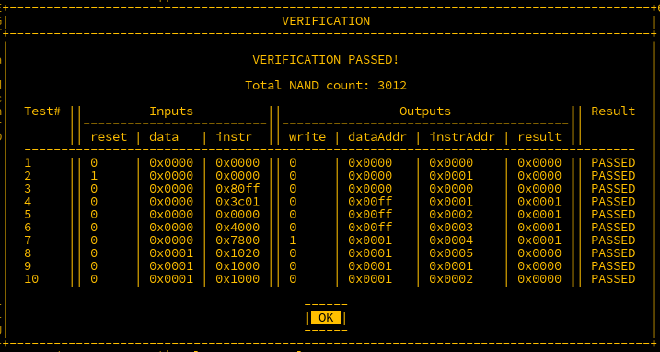
With this complete, the CPU is operational.
Conclusion#
This marks the completion of the MHRD challenge, from building basic gates to constructing a fully functional CPU. While I may revisit this project to explore potential optimisations (such as reducing the NAND count), the core objective has been achieved.
Next up, we’ll tackle similar challenges in a more graphical game, Turing Complete, where we’ll not only build hardware but also write code that can be run on our CPU. I hope you enjoyed this walkthrough.