
Initial#
The next series of components to be crafted are related to the memory, i.e. registers and later on RAM.
Delayed Lines#
This introduces the Delay Line component which takes and input and outputs the bit value one clock tick later. This is identical to the DFF component observed in MHRD.
The challenge asks to take an input and then to output the same value two ticks later. This just requires chaining of two Delay Line components. This unlocks the Delay Line.

Odd Ticks#
Another simple challenge. The goal is to output a 1 every second tick. The trick here is taking the output of a Delay Line, negating it, and feeding it back, so that it will change every tick. The output is also fed to the output.

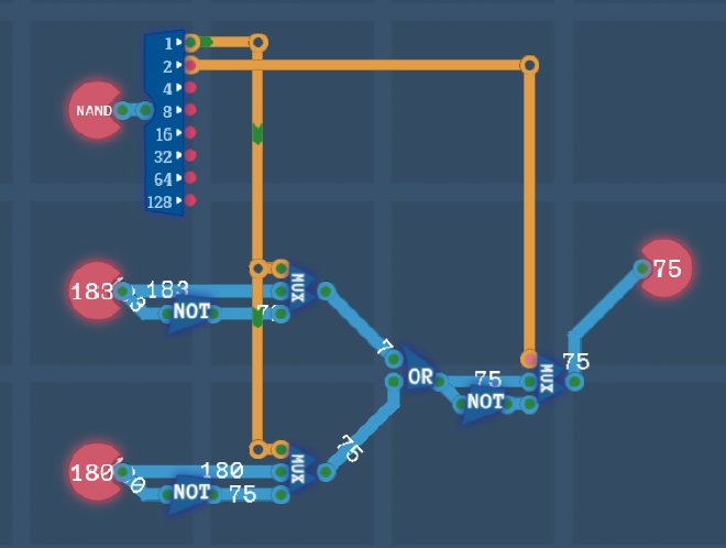
Bit Inverter#
This is just an XOR gate as previously discussed.

Input Selector#
With two inputs A and B, choose which one to send to the output by the value set in the SELECT input. This is just at MUX8B like seen in MHRD.
As we have access to the 8-bit switch component, just connect up the inputs to two switches, and use the SELECT as the enable flag on them, taking not to negate the input of the first switch. This unlocks the MUX component.

The Bus#
Another interesting challenge. There are two inputs, IN 0 and IN 1. The FROM input determines which input to take, and the TO input determines which output to send the input value to. There is a limit of parts to use, just 4 8-bit switch components and 2 NOT gates. The input part is identical to the MUX component just built, and the output part is very similar also. Just be sure to connect the outputs of the first two switches to the last two.

Saving Gracefully#
Looks like the time to build a register has arrived. There are two inputs, ACTION which if enabled means to save the second input VALUE to a Delay Line. The trick to keeping the value stored in the Delay Line is by looping it back on itself as observed before, but this time also allowing to set a new value if requested.
Use two 1-bit switch components and connect the enable to the ACTION input, with one negated. For the negated switch, connect the output of the Delay Line to the input, so if the ACTION is negative, then it will continuously store the value back on itself. If the ACTION is positive however, then the other switch is enabled which outputs the value of the VALUE input.

While we call this component a Register from MHRD, its name here is 1-bit memory which is unlocked. TC’s version of a Register comes next.
Saving Bytes#
Slightly more complex design here. Only store the input value when the SAVE input is set, and only output the stored value when the LOAD input is set.
As there is no way to store a byte, 8 1-bit memory components are used. The input byte is split and fed into each memory piece, and the outputs of the memory pieces are piped back to a Byte Maker. Finally, to handle the LOAD input, this input is connected to the newly added enable flag on the Output. This creates an 8-bit Register.

1 Bit Decoder#
Basic challenge that routes a bit. If the input is negative, then output 1 is postive, otherwise output 2 is. This can all be achived just using a NOT gate. Decoders are useful when using switches. This unlocks the 1-bit Decoder.

3 Bit Decoder#
This is just an extension of the 1-bit Decoder however not as easy. I had originally decided to try this with a series of 1-bit Decoder pieces and a bunch of switches, however in the end I settled for using decoders on the inputs, and piping all permutations into 3-bit AND gates, one for each possible output. This unlocks the 3-bit Decoder.

Little Box#
This challenge provide a new constraint not previously seen before, space. The entirely of this component must fit in a little box. This provides some extra challenges on what components to use and where to try to fit them.
The challenge builds out a 4-byte RAM module. With this of course, these modules can be chained together to make a larger RAM size. Set up 4 Register components, and connect the INPUT to the inputs of the registers. Note that this is safe to so as the registers will only accept the value if the SAVE input is enabled. There are two other inputs that basically state what address to save the value to. The 4 register addresses are A0, A1, B0 and B1 but you can just think of these as 0,1,2,3. My initial idea to solve this was to just use a bunch of 3-bit AND gates to be connected to the LOAD and SAVE inputs, however space did not allow it. Instead, I just used 4 of the ANDs to control input. Each AND gets an input from the two address inputs (or negatives of) and the third input for when the SAVE input is enabled. Due to space, the outputs are handled differently. When the LOAD input is enabled, all registers output however three MUX gates are used to choose which output is requested.
A fun challenge what unlocks a much larger component, a 256 byte RAM.

Counter#
A counter is an extension of a Register in that it stores and hold a value, but also increments by one per tick. This is useful for knowing what address of a program to run for example. There’s an extra contition, that if the SAVE input is set, then the value is overridden by the input value.
Grab a Register, then connect its out value to the output. Also connect the out value to a Full Adder. This will act as the incrementer. Connect the adder output to a MUX so that it can choose between the adder value or the input if overridden. Finally, connect an Always On to the load/save register inputs and the adder carry.

Logic Engine#
The last piece in this section before the CPU building can commence. This should be recognizable as a part of the ALU from MHRD.
There are two byte inputs, and a CODE input that determines what action is to be performed.
0 - OR
1 - NAND
2 - NOR
3 - AND
For logic, there is only one component available at present for bytes, an OR gate. If we remember the Demorgan’s Theorem Graph, these four calculations can be performed by using one gate, just NOT the inputs/outputs to achieve the same effect.
Wiring up the two inputs and the output to the OR gate, it runs as expected of course. To achieve NAND behaviour, the output needs to be swapped using a 8-bit NOT gate. The regular and inverted versions of the output are connecte to a MUX to decide which one to use. This is also performed on both inputs.
To decide what should be flipped when, the CODE is ran through a splitter,and the first bit manages the output, and the second bit manages the two inputs. A basic logic engine is built which also unlocks 8-bit versions of NOR, AND and NAND.
Conclusion#
Registers and RAM are now tackled as well as a basic ALU. Joining these up to the previously created arithmetic components will form a primitive CPU that can be coded for.