
Initial#
The next series of components to be crafted are related to the memory, i.e. registers and later on RAM.
Multiplexer#
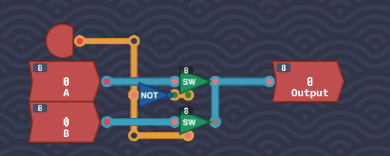
With two inputs A and B, choose which one to send to the output by the value set in the SELECT input. This is just at MUX8B like seen in MHRD.
As we have access to the 8-bit switch component, just connect up the inputs to two switches, and use the SELECT as the enable flag on them, taking not to negate the input of the first switch. This unlocks the MUX component.
The Bus#
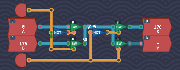
Another interesting challenge. There are two inputs, A and B. The Input Select input determines which input to take, and the Output Select input determines which output to send the input value to. There is a limit of parts to use, just 4 8-bit switch components and 2 NOT gates. The input part is identical to the MUX component just built, and the output part is very similar also. Just be sure to connect the outputs of the first two switches to the last two.
Saving Gracefully#
Looks like the time to build a register has arrived. There are two inputs, Save which if enabled means to save the second input Value to a Delay Line. The trick to keeping the value stored in the Delay Line is by looping it back on itself as observed before, but this time also allowing to set a new value if requested.
Start with a Delay Line as this will be storing our bit. Connect the DL out to Output as expected but also loop it back to a switch. This switch will be enabled when Save is 0 so add a NOT gate from Save to this switch’s enable. As long as ‘Save’ is ‘0’, it will repeat back the value of DL back into itself.
Similar logic applied for the Value input, feed it into a second switch and enable when Save is 1. Pipe both switch outputs to the DL input and you are set.

This unlocks a 1-bit Register.
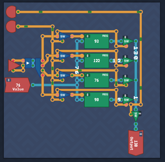
Saving Bytes#
Same design as above but just expanding into 8 bits, so chain up 8 1-bit Registers, connect up the ‘Save’ input as expected, then split/join the input and outputs from bytes to bits.
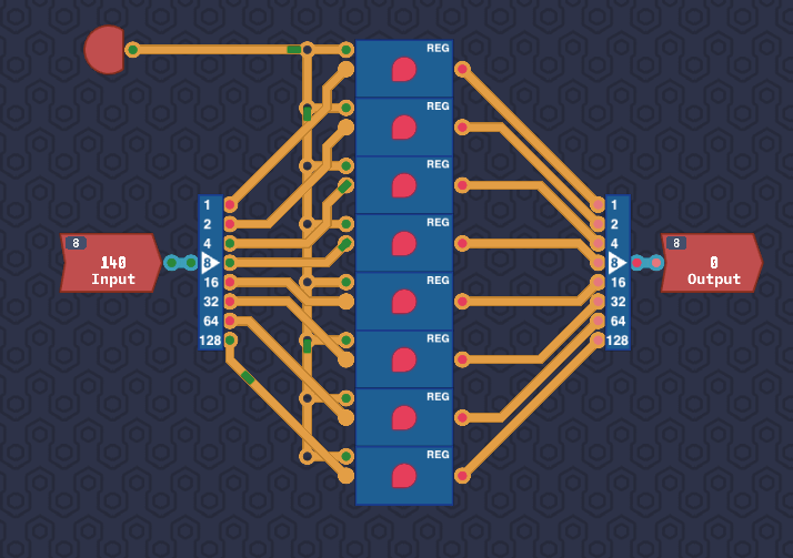
This unlocks our first Register in Turing Complete, and an 8-bit Delay Line.
1 Bit Decoder#
The first in our trio of decoders. Basically think of these are always outputting true on only one output. This couldn’t be simpler, just use a NOT gate.

This unlocks the 1-bit Decoder.
2 Bit Decoder#
A simple extension of this, however we need to use the newly unlocked 1-bit decoders and utilize them with four AND gates. This ensures only one output will ever be true.
3 Bit Decoder#
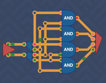
This is just an extension of the 1-bit Decoder however not as easy. I had originally decided to try this with a series of 1-bit Decoder pieces and a bunch of switches, however in the end I settled for using decoders on the inputs, and piping all permutations into 3-bit AND gates, one for each possible output. This unlocks the 3-bit Decoder.
Although it works, I feel like I could tidy this wiring, but if it works….
This unlocks the 3-bit decoder which will come in handy in future.
Arithmetic Logic Unit - 1#
The fun begins finally. All that toil in making the core components is paying off, and this will help us start building out a basic CPU. This should be recognizable as a part of the ALU from MHRD.
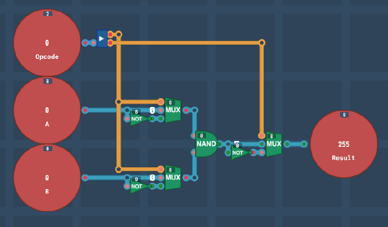
There are two byte inputs, and an OpCode input that determines what action is to be performed.
0 - NAND
1 - OR
2 - AND
3 - NOR
For logic, there is only one component available at present for bytes, a 8-bit NAND gate. If we remember the Demorgan’s Theorem Graph, these four calculations can be performed by using one gate, just NOT the inputs/outputs to achieve the same effect.
Wiring up the two inputs and the output to the NAND gate, it runs as expected of course. To achieve AND behaviour, the output needs to be swapped using a 8-bit NOT gate. The regular and inverted versions of the output are connected to a MUX to decide which one to use. This is also performed on both inputs.
To decide what should be flipped when, the OpCode is ran through a splitter, and the first bit manages the inputs, and the second bit manages the output. A basic logic engine is built which also unlocks 8-bit versions of NOR, AND and OR components.
Little Box#
This challenge provide a new constraint not previously seen before, space. The entirely of this component must fit in a little box. This provides some extra challenges on what components to use and where to try to fit them.
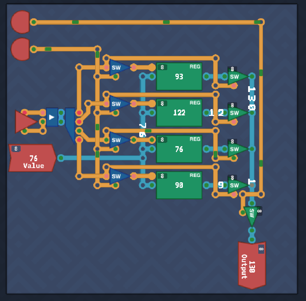
The challenge builds out a 4-byte RAM module. With this of course, these modules can be chained together to make a larger RAM size. Start by setting up 4 Register components named 00, 01, 10, 11. There is a two bit Address input which will select which Register we want to interact with.
There is also a Value input which outputs a byte, and when the Save input is enabled, this value is to be saved to the respective Register. The final input Load is used to output the value of the selected Register. Simple save/load logic.
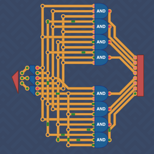
In the older version of TC, I struggled with this a lot, I believe that some parts may have been limited to me but I can no longer check or recall. Below is my old version, where I used a bunch of 3-input AND and MUX gates.
In the newer version of TC, I came at this a different way and in fact it was easy to do. First, add the 4 Register components with a space between them, then hook up the Value input to all. For the address selector, I just piped in both bits in to a 2 bit Maker, then piped that into a 2-bit Decoder which will always select the correct register address. This is then hooked up to switches that enable the save function of the register when the Save input is enabled, then a similar logic for the output. A final switch was added to only output the selected register value when the Load input is on. This is a much more elegant and clean approach.
A fun challenge what unlocks a much larger component, a 256 byte RAM.
Counter#
A counter is an extension of a Register in that it stores and hold a value, but also increments by one per tick. This is useful for knowing what address of a program to run for example. There’s an extra contition, that if the SAVE input is set, then the value is overridden by the input value.
Grab a Register, then connect its out value to the output. Also connect the out value to a Full Adder. This will act as the incrementer. Connect the adder output to a MUX so that it can choose between the adder value or the input if overridden. Finally, connect an Always On to the load/save register inputs and the adder carry.
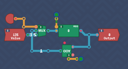
This unlocks the Counter component.
Conclusion#
Registers and RAM are now tackled as well as a basic ALU. Joining these up to the previously created arithmetic components will form a primitive CPU that can be coded for.