
Introduction#
With the foundations now in place, it’s time to build our first CPU—capable of receiving and executing instructions. Unlike in MHRD, here we have the flexibility to craft our own instruction set. While it may be basic initially, the CPU will be of our own design and creation.
Arithmetic Logic Unit - 2#
We begin by enhancing the previous ALU design by adding ADD and SUB functionalities. While it’s possible to use De Morgan’s laws and rely on a single logic gate for the first four operations, it’s cleaner and more efficient to use the newly unlocked gates.
As the splitter only handled two bit inputs, I replaced it with a 4-bit splitter. When the third bit is enabled, it switches to the ADD/SUB output. I added a MUX to handle this bit.
Next, add an Adder that takes input A and a MUX that is used a Negate to take the value of B and either pipe B as normal (ADD) or a negated version (SUB) using the Negate output.
This was just a simple addition but a basic ALU is now built.
Overture Architecture#
We are now ready to build our first CPU architecture: Overture. Unlike previous challenges, this design will be refined over time, and improvements will carry over to earlier challenges when revisited. This will also be a LOT of fun.
Registers#
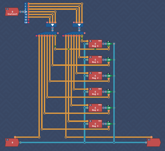
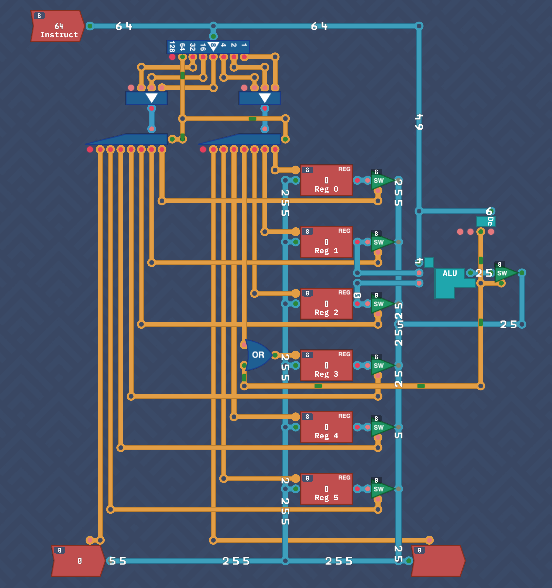
The architecture starts with three key components: Instruction, INPUT, and OUTPUT, along with six Register components named REG 0 to REG 5.
At this stage, the instruction set is simple: values are copied from one location to another. The three lowest bits of the instruction specify the destination, while the next three bits indicate the source. The two highest bits are unused for now.
Here’s how the inputs and outputs map to the instruction bits:
000 - REG 0
001 - REG 1
010 - REG 2
011 - REG 3
100 - REG 4
101 - REG 5
110 - Input/Output
For instance, to store the value from INPUT into REG 3, the instruction would look like XX 110 011 (the XX representing the ignored two highest bits).
Since only one source and one destination are used at a time, all inputs and outputs are connected together, with a Switch connected to the output of each register.
Split the Instruction input with a Splitter. Feed the three source and destination bits into a Maker each and the outputs of the makers into a 3-bit Decoder. This will act as the selector of what we want to input/output from.
The input decoder will enable a Register to load an input or load from the Input itself. The output decoder will enable a register output switch or the Output as the destination
I actually found it very useful to run the simulation until it reached an error, then connect the correct input/output selectors one by one until it completed.
Instruction Decoder#
The remaining two bits of the instruction determine the action to be performed. At this point, the CPU can only COPY values from one place to another. As additional functionality is added, these bits will drive more complex operations. For now, here are the possible values:
00 - IMMEDIATE
01 - CALCULATE
10 - COPY
11 - CONDITION
This is a simple grabbing of the two remaining bits and running them through a maker and decoder.
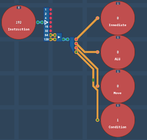
Other operations will be introduced as new components are added.
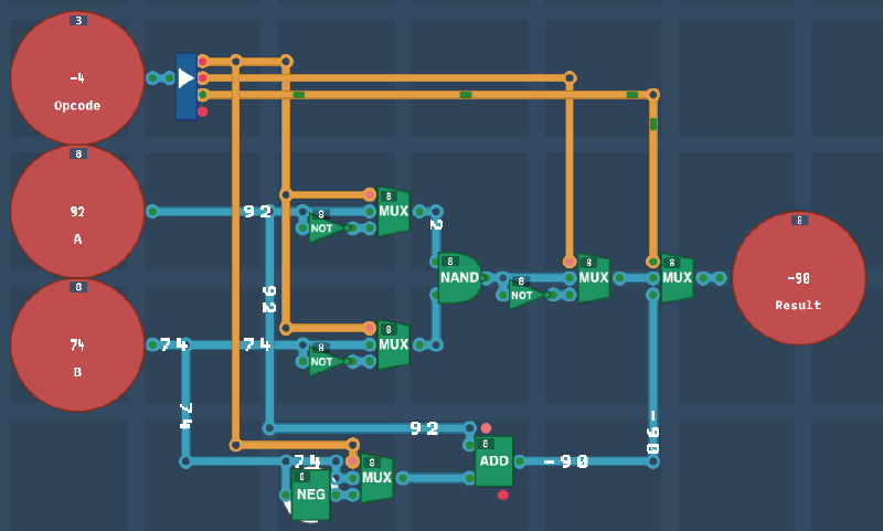
ALU#
This brings our freshly designed ALU and Dec components back into the registers schematic. The notes state the following two modes are now possible:
ALU - Perform ALU calculation
MOVE - Move data from input -> output (Already completed)
The notes also state that when in ALU mode, to take the values of REG 1 and REG 2 as inputs, and store the output of the ALU into REG 3.
I placed the ALU to the right of the input registers and fed their values into the ALU. Next, I added the Dec module and connected it to the a switch that handles the ALU output which will only output back to the byte circuit when true. Reg 3 however needs to be told to take a value so I added an OR gate to handle the move bit as well as the ALU calculation output.
d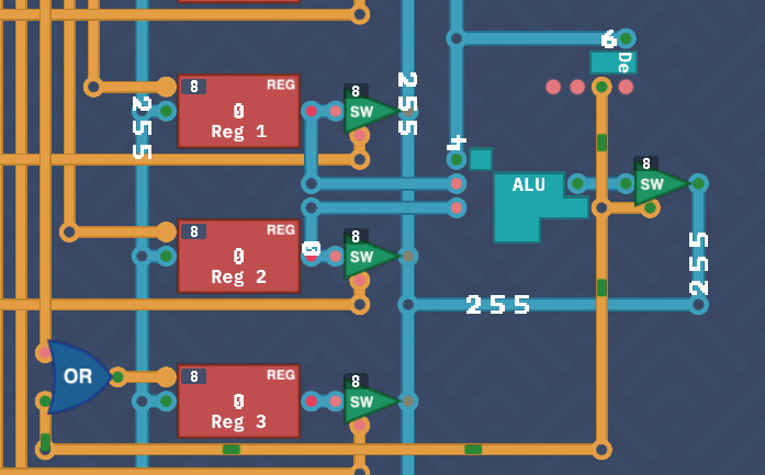
The ALU OpCode is the lower bits of the Instruction input, so that is fed into it also.
To avoid unwanted behavior, the decoders (used during MOVE operations) can be disabled during other operations by adding an additional control signal. This is managed by connecting the 7th bit of the instruction splitter to the decoder disable pins, ensuring they are only active during a COPY.
To summarize, for all ALU operations, REG 1 provides the first input, REG 2 the second, and REG 3 stores the result. At this point, the Overture CPU can handle both MOVE and ALU instructions.
Conditions#
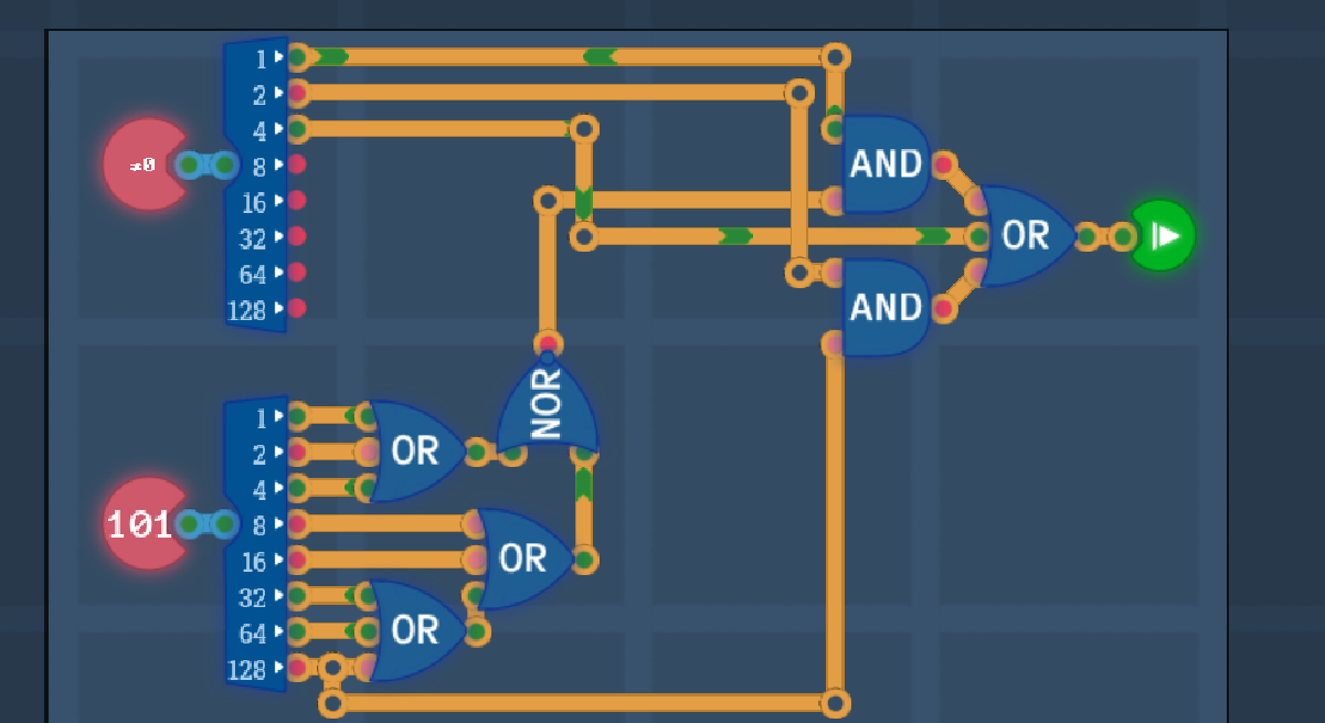
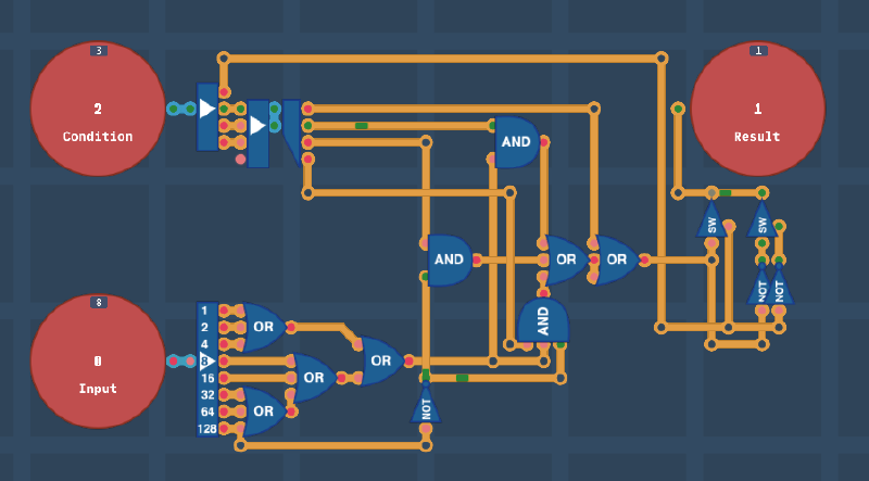
Conditional operations are the next step, though the component required for this hasn’t been designed yet. The goal is to check specific conditions, such as whether a value is zero, positive, negative, etc.
This component took some trial and error to design, but the solution became clear as I focused on building one condition at a time. Here’s how the conditions were implemented.
The OpCodes are:
000 (0) - Never
001 (1) - Always
010 (2) - If value == 0
011 (3) - If value != 0
100 (4) - If value < 0
101 (5) - If value >= 0
110 (6) - If value <= 0
111 (7) - If value > 0
Let’s think about this. Ignoring the first two for now, all compare the value to a relationship of zero. Also, if you close closely, they are four pairs of opposites with the least significant bit toggling between them.
Start by splitting the bits of the input and chaining them together with multiple OR gates. This will determine if it is zero of not.
Next, build a bit flipper using two switches and NOT gates. I would’ve used a MUX however they were not available. This will be controlled by the LSB of the condition making the opposite of the input if it is true.
Next chain up an OR and a 3-bit OR gate so that it can take four inputs, one for each condition.
Finally, with the remaining 3 bits from the condition, feed into a decoder.

Always/Never True#
This is the simplest logic. Just feed decoder bit 1 into the first OR input.
Value =0 or !=0#
Add an AND gate to take the decoder bit 2 and the output of the input OR gates. Feed into the second OR gate input.
Value <0 or >=0#
This is very simple and similar to the above, just one AND gate taking decoder bit 3 and the negative bit from input negated.
Value <=0 or > 0#
This is slightly more complex where it requires a three input AND gate that’s a combination of the above two conditions. It takes the final decoder bit, the negated negative bit and the input OR gates.
This was my solution but I get the feeling there’s a more efficient approach. I’ll return to this in the future but overall this is efficient and elegant enough for me.
Conclusion#
The Overture CPU design is nearing completion. In the next section, we’ll finalize the design and take the first steps toward writing code that can execute on this CPU.